
Growth Mechanism And Physical Properties Of The Type I In0 145ga0 855asysb1 Y Gasb Alloys With Low As Content For Near Infrared Applications Sciencedirect


Electrical Modeling Of Inas Gasb Superlattice Mid Wavelength Infrared Pin Photodiode To Analyze Experimental Dark Current Characteristics Journal Of Applied Physics Vol 116 No 11

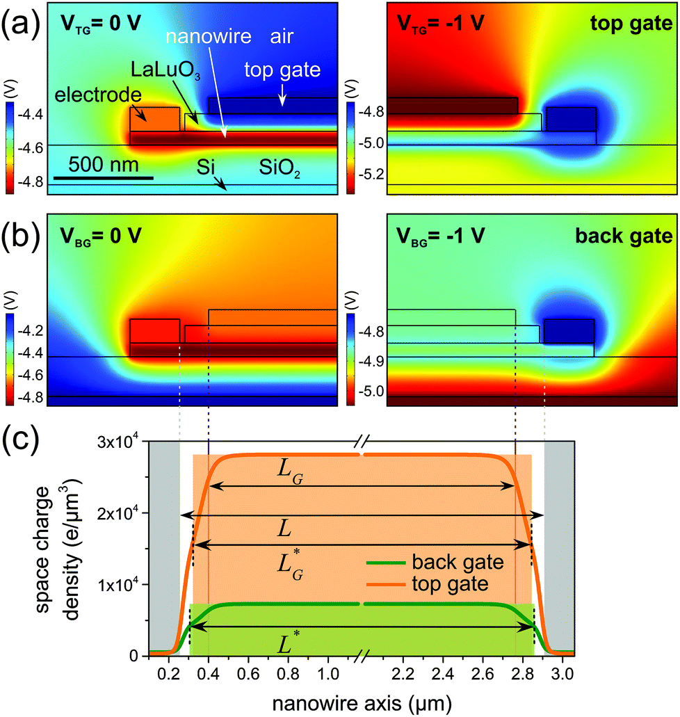
Resolving Ambiguities In Nanowire Field Effect Transistor Characterization Nanoscale Rsc Publishing Doi 10 1039 C5nr03608a


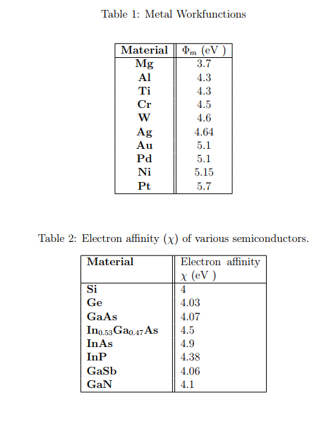
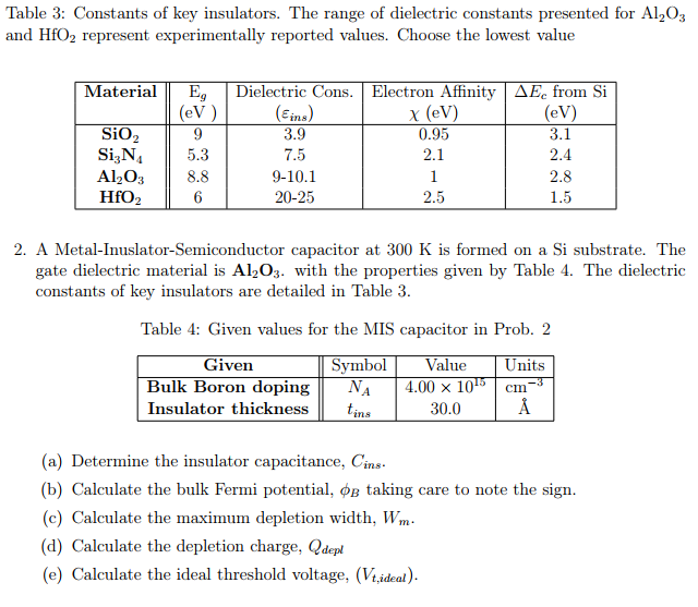

Table 2 From Investigation And Simulation Of Work Function Variation For Iii V Broken Gap Heterojunction Tunnel Fet Semantic Scholar

Solution Processed Inas Nanowire Transistors As Microwave Switches Mirkhaydarov 2019 Advanced Electronic Materials Wiley Online Library


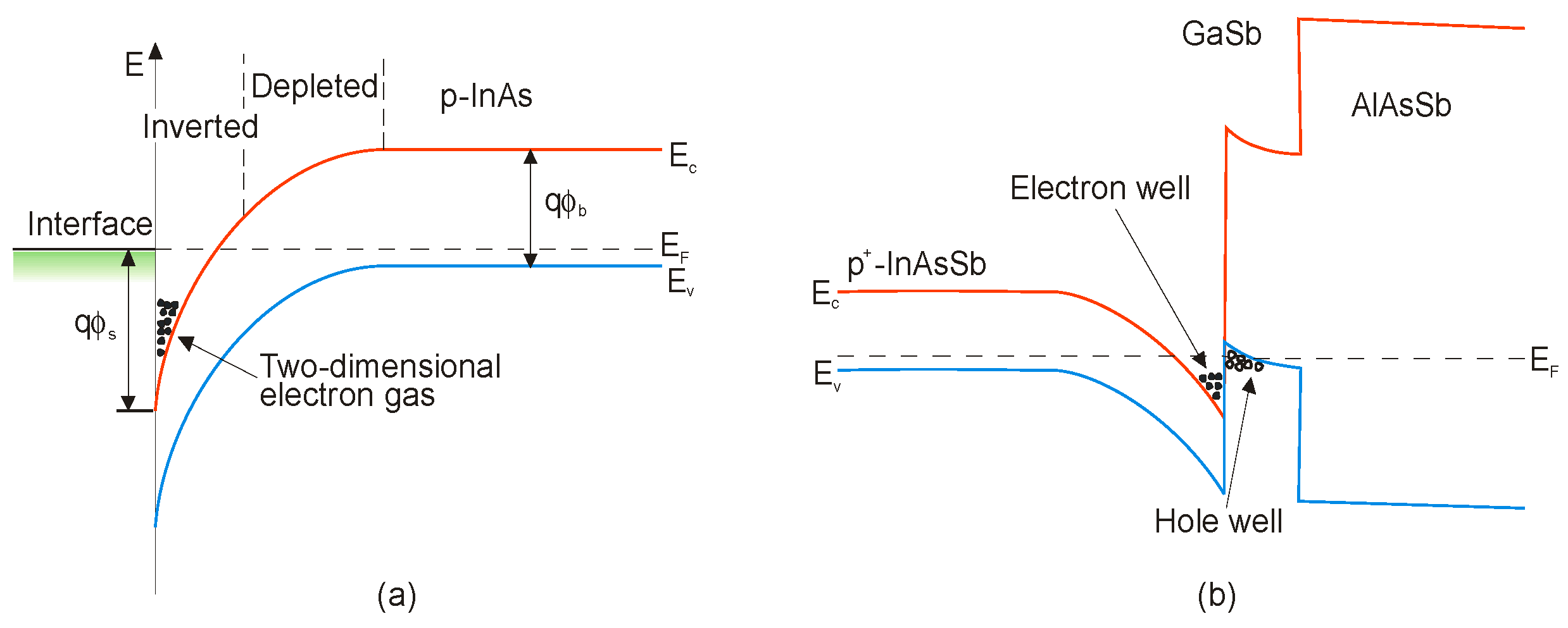
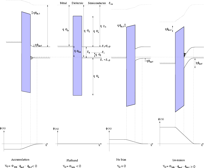
Band Offsets Schottky Barrier Heights And Their Effects On Electronic Devices Journal Of Vacuum Science Technology A Vol 31 No 5
No comments:
Post a Comment